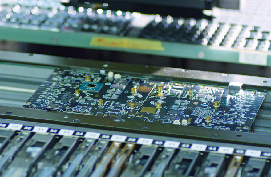
PCB Manufacturing Solderability Design
It needs to be coated on the surface of the PCB after the pcb board is etched, . There are two main aspects in this method:

1. Coating a solder mask on the non-soldering area of the pcb circuit board, which can prevent the solder from flowing thereby causing bridging connection and affecting the moisture resistance of the pcb after soldering.
2. Coating on the pcb manufacturing pad to prevent pad oxidation and improve solderability.
(1) Solder Mask coating. The solder mask is typically a thermally or photocurable resin such as propylene resin, epoxy Resin, silicone, etc. Solder mask coating can be divided into dry film method and wet film method. The dry film method refer to a film made of a certain thickness which is coated on a PCB circuit board, and then the pad portion is exposed by photolithography. The wet film method is to print liquid photoimageable solder mask on a PCB integrally , and then expose the pad portion by photolithography. The fenestration dimensional accuracy of the solder mask depends on the level of the PCB manufacturer's craft.
(2) Pad coating. The printed circuit board pads are made of metallic copper, which has excellent solderability, but in acid-containing humid air, the copper surface is oxidizabled easily. Thus the solderability is lost. In order to prevent or delay the process of poor solderability, the surface of the copper must be properly coating.
The above is the surface coating design of pcb solderability, I hope it’s helpful to you.
Article keywords :PCB,Manufacturing,Solderability,Design,needs,coated,the,


 2021-07-26 06:14:22

